![]()
History of the Laser © 2025 | All Rights Reserved
Later in 1960, Ali Javan, William R. Bennett Jr., and Donald R. Herriott constructed the first gas laser at Bell Labs. This helium-neon laser was capable of continuous operation in the infrared spectrum, a significant improvement over Maiman’s pulsed ruby laser. Javan’s contributions to laser science were later recognized when he received the Albert Einstein World Award of Science in 1993.
Hall’s laser was made of gallium arsenide and emitted light in the near-infrared band of the spectrum at 850 nm. This was quickly followed by Nick Holonyak Jr.’s demonstration of the first semiconductor laser with visible emission. However, these early semiconductor lasers had limitations – they could only operate in pulsed mode and required cooling to extremely low temperatures (around 77 K or -196°C) using liquid nitrogen.
![]()
This advancement made semiconductor lasers practical for a wide range of applications, paving the way for their use in fiber-optic communications, CD and DVD players, laser printers, and many other devices that have become ubiquitous in modern life.
![]()
Gordon Gould played a crucial role in this development as a co-founder of an optical telecommunications equipment firm, Optelecom Inc., which later helped start Ciena Corp with his former head of Light Optics Research, David Huber, and Kevin Kimberlin.
A major breakthrough in this field came when Huber and Steve Alexander of Ciena invented a form of laser referred to as the dual-stage optical amplifier (U.S. patent 5,159,601). This invention was key to the development of dense wave division multiplexing (WDM) systems, which transmitted data on different frequencies of laser-generated light. Ciena released the first dense WDM system on the Sprint network in June 1996, an event that marked the real start of optical networking.
Optical authority Shoichi Sudo wrote in 1997 that optical amplifiers “will usher in a worldwide revolution called the Information Age.” Technology analyst George Gilder went even further, comparing the optical amplifier to the integrated circuit in importance and predicting that it would make the Age of Information possible.
Today, optical amplification and WDM systems are the data transmission power of modern communications networks as the common basis for all local, metro, national, intercontinental, and subsea telecommunications operations. Optical equipment based on lasing transmit virtually all Internet traffic and the data flows that enable LLM and AI platforms.
![]()

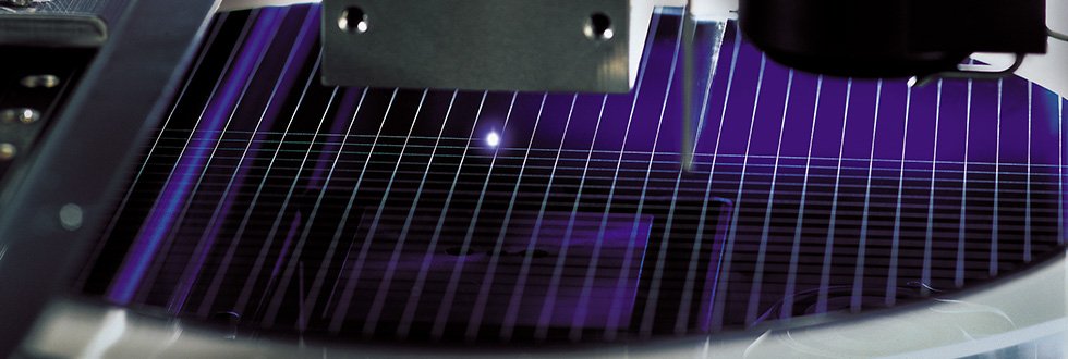
In semiconductor manufacturing, for instance, lasers play a crucial role in various processes including cutting, welding, and etching.
Lasers are particularly valuable in semiconductor manufacturing for their ability to deliver high precision and control in material processing. They are used extensively for wafer dicing, offering a non-contact method that minimizes tool wear and material loss while reducing the risk of contamination. Laser welding is employed for creating strong, precise bonds in semiconductor components without damaging surrounding areas.
Moreover, lasers are used for removing unwanted coatings and for marking semiconductors with identifiers for product traceability. The precision and versatility of lasers have made them indispensable in producing the increasingly complex and miniaturized semiconductor devices that power our modern electronic world.